How Transistors Work: Semiconductors, Doping, and MOSFETs Explained
Learn how transistors work inside CPUs, from silicon and semiconductor doping to N-type, P-type, MOSFET channels, binary logic, and transistor history.
A modern processor contains an enormous number of microscopic electronic switches called transistors. By controlling electrical signals, these switches form logic gates, memory cells, arithmetic circuits, and ultimately the hardware that executes software.
This chapter explains how transistors work from the ground up. We will begin with voltage, current, and digital logic before exploring silicon, semiconductor doping, N-type and P-type materials, and the operation of an N-channel MOSFET. We will finish with a short history of the technologies that made modern computing possible.
What Is a Transistor?
A transistor is a semiconductor device that can control electrical current or voltage. Depending on how it is used, it can act as:
- an electronic switch;
- a signal amplifier;
- a current or voltage regulator.
Digital computers primarily use transistors as switches. A transistor can create a low-resistance path in one state and a high-resistance path in another. Circuits interpret the resulting voltage levels as binary values such as 0 and 1.
It is useful to be precise here: a transistor is not automatically a bit, and the absence of current does not always mean binary 0. Engineers define voltage ranges that count as logical low and logical high. Multiple transistors are then connected to build logic gates, registers, memory cells, and processing units.
The word bit is short for binary digit: one of two possible logical values.
Electricity Basics: Voltage, Current, and Resistance
Before examining semiconductor physics, it helps to understand three electrical quantities.
Voltage
Voltage is the difference in electric potential between two points. It represents the energy available to move electric charge through a circuit.
Voltage is measured in volts, written as V.
A water-pressure analogy can be helpful: a larger pressure difference can push water through a pipe more strongly. The analogy is not perfect, but it gives an intuitive picture of why voltage must be measured between two points.
Current
Current is the rate at which electric charge moves through a circuit.
Current is measured in amperes, written as A.
In a metal wire, current is associated with the movement of electrons. Conventional current is defined as flowing in the direction positive charge would move, which is opposite to the direction of electron movement.
Resistance
Resistance describes how strongly a material or component opposes current.
Resistance is measured in ohms, written as Ω.
A transistor used as a digital switch does not behave exactly like a mechanical switch. Instead, it changes the conductivity of a path. In its on state, the path has relatively low resistance. In its off state, the path has very high resistance, although a small leakage current can still exist.
How Electrical Signals Represent Binary Values
Digital circuits use ranges of voltages to represent binary states:
- Logical low represents
0. - Logical high represents
1.
These states are not universal voltage values. A logical high might be close to 5 V, 3.3 V, 1.2 V, or another level depending on the technology.
Digital circuits also use thresholds. A voltage below one threshold is interpreted as low, while a voltage above another threshold is interpreted as high. The separation between those ranges helps circuits tolerate a limited amount of electrical noise.
This means binary logic is based on how circuits interpret voltage levels, not simply on whether current exists.
What Is a Semiconductor?
A semiconductor is a material whose electrical behaviour lies between that of a conductor and an insulator.
- Conductors such as copper contain many mobile charge carriers and allow current to flow easily.
- Insulators such as glass or plastic strongly resist the movement of charge.
- Semiconductors can be engineered so their conductivity changes in a controlled way.
Silicon is the most widely used semiconductor material in digital electronics. It is abundant, can be purified to a high degree, forms a useful insulating oxide, and can be manufactured into extremely small structures.
Why Pure Silicon Conducts Poorly
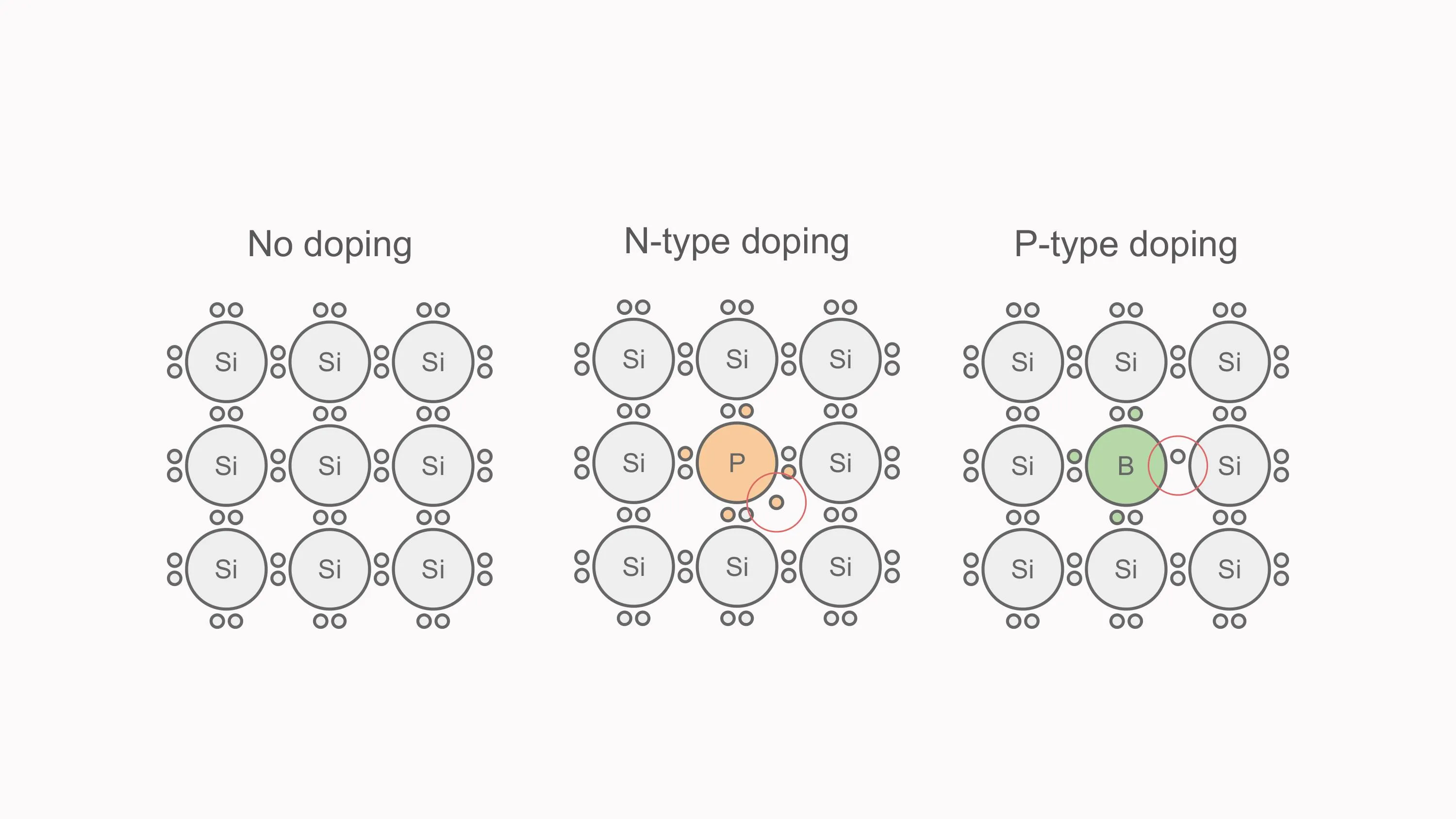
A silicon atom has four valence electrons in its outer electron shell. In a silicon crystal, each atom shares electrons with neighbouring atoms through covalent bonds.
At very low temperatures, most of these electrons remain bound in the crystal structure. At ordinary temperatures, thermal energy allows a limited number of electrons to break free and enter a state where they can move through the material.
When an electron leaves a bond, it creates an empty state called a hole. Nearby electrons can move into that empty state, making the hole appear to travel through the crystal.
Pure, undoped silicon is called an intrinsic semiconductor. It contains some mobile electrons and holes, but not enough for most electronic devices. Engineers change its electrical properties through a process called doping.
What Is Semiconductor Doping?
Doping is the controlled introduction of a small quantity of impurity atoms into a semiconductor crystal.
The word impurity does not mean accidental contamination. The dopant atoms are deliberately selected and precisely controlled during manufacturing.
Doping changes the number and type of mobile charge carriers in the material. Silicon can be turned into either:
- an N-type semiconductor, in which electrons are the majority carriers;
- a P-type semiconductor, in which holes are the majority carriers.
The letters refer to the dominant mobile charge carriers:
Nrefers to negative electrons;Prefers to positive holes.
The complete material remains electrically neutral overall. N-type silicon is not simply a negatively charged block, and P-type silicon is not simply a positively charged block.
N-Type vs P-Type Semiconductors
The difference between N-type and P-type silicon comes from the dopant atoms added to the crystal.
| Property | N-type silicon | P-type silicon |
|---|---|---|
| Common dopant | Phosphorus or arsenic | Boron |
| Dopant valence electrons | Five | Three |
| Majority carrier | Electrons | Holes |
| Minority carrier | Holes | Electrons |
| Dopant role | Donor | Acceptor |
N-Type Doping
Silicon has four valence electrons. A phosphorus atom has five.
When phosphorus replaces a silicon atom in the crystal, four of its electrons participate in bonds with neighbouring silicon atoms. The fifth electron is only weakly bound and can move through the material more easily.
Phosphorus therefore acts as a donor, because it contributes an electron that can become a mobile charge carrier.
The added mobile electrons make the material N-type.
P-Type Doping
A boron atom has three valence electrons.
When boron replaces a silicon atom, one of the four expected bonds lacks an electron. This missing electron creates a hole that can move through the crystal as neighbouring electrons change bonds.
Boron acts as an acceptor, because it can accept an electron into the incomplete bond.
The mobile holes make the material P-type.
How P-Type and N-Type Regions Create Electronic Devices
The ability to place differently doped regions next to one another makes semiconductor devices possible.
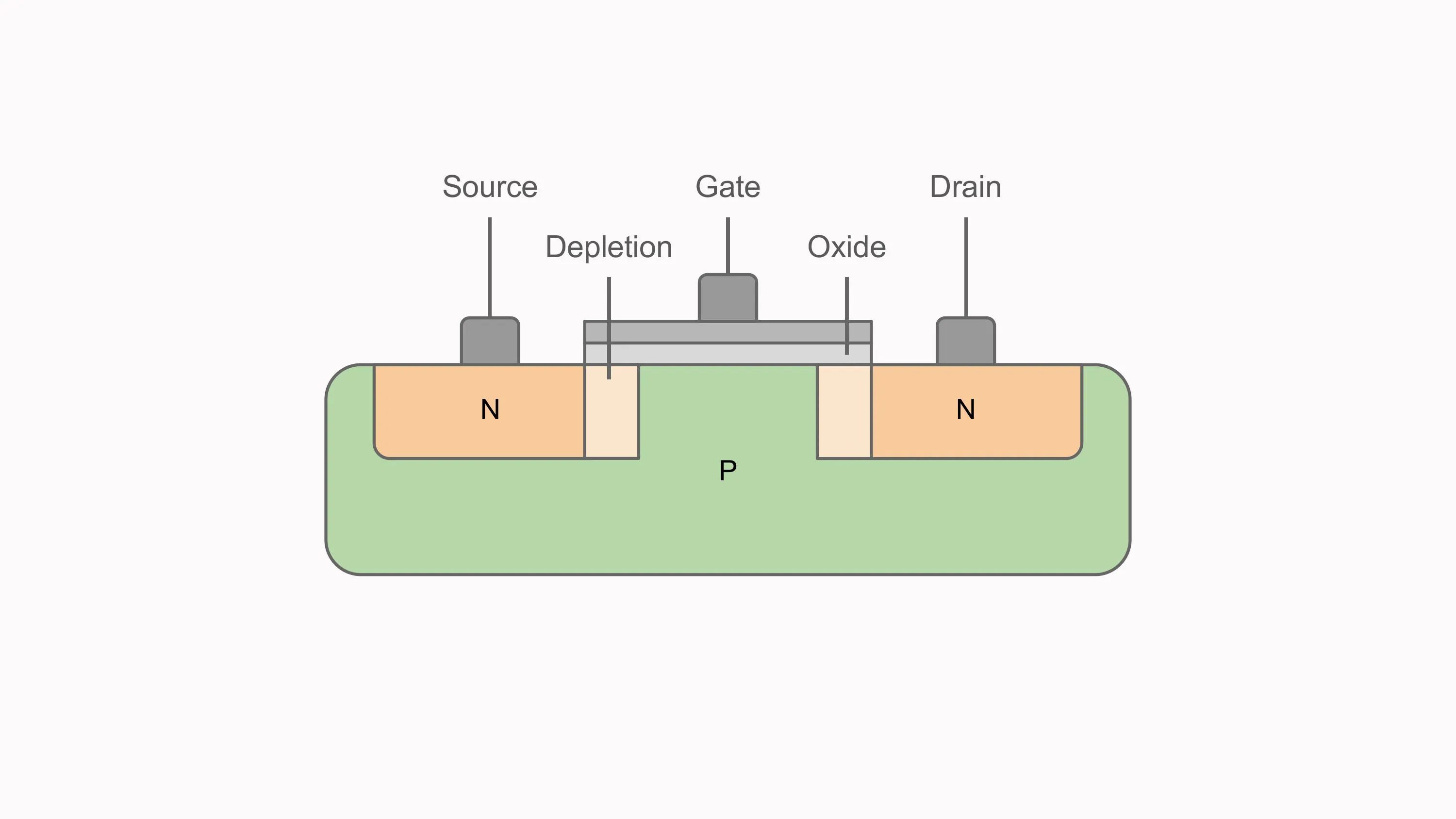
When P-type and N-type material meet, electrons and holes initially diffuse across the boundary and recombine. This leaves a region containing fixed ionized dopant atoms but few mobile carriers.
That carrier-poor area is called the depletion region. It creates an internal electric field and an energy barrier that affects whether current can cross the junction.
A P-N junction is the foundation of a diode and is also important in bipolar transistors. A MOSFET uses doped regions too, but its switching action is controlled primarily by an electric field created by an insulated gate.
What Is a MOSFET?
A MOSFET, or metal-oxide-semiconductor field-effect transistor, is a voltage-controlled transistor with an electrically insulated gate.
MOSFETs are especially important in digital electronics because they can be made extremely small and require very little steady-state gate current. Modern processors use complementary pairs of N-channel and P-channel MOSFETs in a circuit style called CMOS.
This chapter focuses on a simplified enhancement-mode N-channel MOSFET, commonly called an NMOS transistor.
The Four Parts of an NMOS Transistor
A MOSFET is often discussed as a three-terminal device, but its physical structure has four terminals:
- Gate: controls the conductivity of the channel.
- Source: supplies the mobile charge carriers.
- Drain: receives the carriers after they cross the channel.
- Body or bulk: the semiconductor substrate in which the device is formed.
In many circuits, the body is connected internally to the source, which is why simplified diagrams often show only the gate, source, and drain.
A basic enhancement-mode NMOS transistor contains:
- two heavily doped N-type regions for the source and drain;
- a P-type body between them;
- a gate electrode above that region;
- a thin insulating layer between the gate and semiconductor.
Traditionally, the insulating layer was silicon dioxide. Modern transistors may use more advanced materials, but the operating principle remains based on an insulated gate controlling an electric field.
How an NMOS Transistor Works
An NMOS transistor switches by using the gate voltage to create or remove a conductive channel between the source and drain.
The Off State
When the gate-to-source voltage, written as V_GS, is zero or too low, the P-type region under the gate does not contain a continuous N-type channel.
The N-type source and drain are therefore separated by the P-type body. The source-body and drain-body boundaries form P-N junctions, and no low-resistance path connects source to drain.
The transistor is considered off, although real devices still allow a very small leakage current.
Applying a Positive Gate Voltage
The gate is separated from the semiconductor by an insulating layer, so charge does not normally flow directly from the gate into the channel.
Instead, a positive gate voltage creates an electric field through the insulator. This field:
- repels positively charged holes from the surface below the gate;
- attracts electrons toward that surface;
- changes the carrier concentration in the region between source and drain.
At first, the surface becomes depleted of holes. As the gate voltage increases further, enough electrons gather near the surface to make it behave like N-type material.
This electron-rich surface is called an inversion layer.
The Threshold Voltage
The gate-to-source voltage at which a conducting inversion channel begins to form is called the threshold voltage, written as V_TH.
Below the threshold, the transistor conducts only weakly.
Above the threshold, a channel connects the N-type source and drain regions. If a voltage also exists between drain and source, current can flow through that channel.
The threshold voltage marks the beginning of significant channel formation. It should not be confused with the voltage required to make a real power MOSFET conduct its maximum rated current.
The On State
When the gate voltage is sufficiently above the threshold, the inversion layer forms a relatively conductive path between source and drain.
The transistor is then considered on.
For an NMOS device:
- electrons physically move through the channel from source toward drain;
- conventional current is defined in the opposite direction, from drain toward source.
The gate voltage also affects the conductivity of the channel. A stronger gate electric field attracts more electrons, reducing the channel resistance within the device’s safe operating range.
A Simple MOSFET Analogy
You can imagine the gate as controlling the construction of a temporary bridge.
- With insufficient gate voltage, no continuous bridge connects the source and drain.
- Once the gate voltage crosses the threshold, an electron channel forms beneath the gate.
- A drain-to-source voltage can then drive current through that channel.
This analogy is more accurate than imagining a physical gate that mechanically opens. Nothing inside the MOSFET moves like a door or lever. The conductive path appears because an electric field rearranges charge carriers in the semiconductor.
Why MOSFETs Work Well as Digital Switches
A MOSFET gate is insulated, so ideally it does not require a continuous input current to remain in one state. However, the gate behaves partly like a tiny capacitor and must be charged or discharged whenever the transistor switches.
This gives digital circuits two important characteristics:
- relatively low static power consumption;
- energy consumption during switching.
Real MOSFETs are not perfect switches. They have channel resistance, capacitance, leakage, propagation delay, and voltage limits. Computer engineers must account for all of these effects when designing fast and efficient processors.
From MOSFETs to CMOS Logic
A single transistor is useful, but computation emerges when many transistors are connected together.
Modern digital chips primarily use CMOS, which stands for complementary metal-oxide-semiconductor. CMOS circuits combine:
- NMOS transistors, which are effective at pulling a signal toward a low voltage;
- PMOS transistors, which are effective at pulling a signal toward a high voltage.
The simplest CMOS logic gate is an inverter, also called a NOT gate. It uses one PMOS and one NMOS transistor:
- when the input is low, the PMOS turns on and the output becomes high;
- when the input is high, the NMOS turns on and the output becomes low.
More transistors can be arranged into NAND, NOR, AND, OR, XOR, and other logic functions. Those gates become adders, multiplexers, registers, caches, control units, and processor cores.
The key idea is that a CPU does not perform computation with isolated transistors. It performs computation through carefully designed networks of transistors that transform electrical signals according to Boolean logic.
From Vacuum Tubes to Transistors
Before solid-state transistors, electronic computers used vacuum tubes.
A vacuum tube controls the movement of electrons through an evacuated glass or metal enclosure. Tubes made electronic amplification and high-speed switching possible, but they were physically large, consumed substantial power, generated heat, and had limited lifetimes.
Early electronic computers therefore occupied large rooms and required extensive cooling and maintenance.
The First Transistor
In December 1947, John Bardeen and Walter Brattain demonstrated the first successful point-contact transistor at Bell Laboratories. William Shockley led the research group and subsequently developed the junction-transistor concept.
The work of Shockley, Bardeen, and Brattain established the transistor as a practical solid-state alternative to vacuum tubes. The three researchers received the 1956 Nobel Prize in Physics for their semiconductor research and discovery of the transistor effect.
The Invention of the MOSFET
The MOSFET followed more than a decade later.
Mohamed Atalla and Dawon Kahng built the first successful MOS field-effect transistor at Bell Laboratories in 1959 and presented the device publicly in 1960. Their work depended on improvements to the silicon-silicon-dioxide interface, which made it possible for an insulated gate to control the semiconductor surface reliably.
The MOSFET was initially slower to gain commercial attention than some other transistor designs. Its ability to scale to small dimensions, consume little static power in CMOS circuits, and support dense manufacturing eventually made it the dominant transistor technology for digital integrated circuits.
Why Transistors Became the Foundation of Modern Computing
Compared with vacuum tubes, transistors offered major advantages:
- much smaller physical size;
- lower operating voltage;
- lower power consumption;
- less heat generation;
- greater reliability;
- faster switching;
- easier integration into mass-produced circuits.
A single transistor cannot perform the work of a computer. The breakthrough came from manufacturing many transistors and their connections on one semiconductor chip.
As fabrication techniques improved, engineers could place increasingly complex circuits on integrated circuits. That progression led from simple logic chips to memory devices, microcontrollers, graphics processors, and modern CPUs.
Common Misconceptions About Transistors
A Transistor Is Not Literally a Binary Digit
A transistor is a physical device. A bit is an abstract binary value. Circuits use one or more transistors to represent, store, or process bits.
Off Does Not Mean Absolutely No Current
Real transistors leak a small amount of current even when they are nominally off. Leakage becomes increasingly important as devices become smaller.
The Gate Does Not Supply the Main Channel Current
The insulated gate creates the electric field that controls the channel. The main current travels between the source and drain.
N-Type Does Not Mean the Material Has a Net Negative Charge
N-type silicon has electrons as its majority mobile carriers, but the material remains electrically neutral overall.
P-Type Is Not Made with Phosphorus
The chemical symbol for phosphorus is uppercase P, but phosphorus is commonly used to create lowercase n-type silicon because it donates electrons. Boron is commonly used to create p-type silicon because it creates holes.
Frequently Asked Questions
How does a transistor work inside a CPU?
A CPU uses MOSFETs as voltage-controlled switches. Networks of NMOS and PMOS transistors form logic gates. Those gates are combined into arithmetic circuits, registers, memory structures, and control logic that process machine instructions.
What is the difference between N-type and P-type silicon?
N-type silicon has electrons as its majority carriers and is commonly produced by adding donor atoms such as phosphorus. P-type silicon has holes as its majority carriers and is commonly produced by adding acceptor atoms such as boron.
What does the gate of a MOSFET do?
The gate creates an electric field through an insulating layer. In an enhancement-mode NMOS transistor, a sufficiently positive gate-to-source voltage attracts electrons to the semiconductor surface and forms a conductive channel between source and drain.
Does current flow into a MOSFET gate?
Ideally, no steady direct current flows through the insulated gate. In practice, a small leakage current may exist, and current is required briefly to charge or discharge the gate capacitance during switching.
Why is silicon used for transistors?
Silicon is abundant, can be purified and processed accurately, has useful semiconductor properties, and forms a stable oxide that has been essential to MOS technology.
Are all transistors MOSFETs?
No. Other transistor families include bipolar junction transistors, junction field-effect transistors, and specialized high-frequency or power devices. MOSFETs dominate modern digital integrated circuits.
What is the difference between a transistor and a logic gate?
A transistor is an individual electronic device. A logic gate is a circuit made from multiple transistors that implements a Boolean operation such as NOT, NAND, or NOR.
Key Takeaways
A transistor is a semiconductor device that can control an electrical signal. In digital circuits, MOSFETs act as switches whose state depends on voltage.
The essential ideas are:
- Pure silicon has limited conductivity.
- Doping changes the concentration of mobile charge carriers.
- Phosphorus commonly creates N-type silicon with mobile electrons.
- Boron commonly creates P-type silicon with mobile holes.
- An NMOS gate uses an electric field to form an inversion channel.
- CMOS combines NMOS and PMOS transistors to build efficient logic gates.
- Networks of those gates form the functional parts of a processor.
The transistor is the first step in understanding computer architecture. The next step is learning how several transistors are connected to create logic gates that can make decisions using binary signals.