How Logic Gates Work: Build an 8-Bit Binary Adder and Memory Circuit
Learn how logic gates work, build half-adders and full-adders, create an 8-bit ripple-carry adder, and understand latches, flip-flops, and memory.

Transistors become useful for computing when they are connected into logic gates. These gates transform binary input signals into binary outputs, making it possible to compare values, perform arithmetic, store information, and control the flow of data inside a processor.
In this chapter, we will move from individual transistor switches to complete digital circuits. We will study the NOT, AND, OR, XOR, NAND, and NOR gates, build a half-adder and full-adder, combine eight full-adders into an 8-bit ripple-carry adder, and finish with an introduction to sequential logic, latches, flip-flops, and one-bit memory.
What You Will Learn
By the end of this chapter, you will understand:
- how digital circuits interpret low and high voltage levels;
- how truth tables describe logic-gate behaviour;
- what NOT, AND, OR, XOR, NAND, and NOR gates do;
- the difference between combinational and sequential logic;
- how a half-adder adds two binary digits;
- how a full-adder includes a carry-in value;
- how eight full-adders create an 8-bit adder;
- why carry-out and signed overflow are not the same;
- how feedback allows a circuit to remember one bit;
- the difference between a latch and a flip-flop.
From Transistors to Logic Gates
In the previous chapter, we saw that a transistor can behave like an electronically controlled switch. A control signal changes whether the transistor provides a relatively low-resistance or high-resistance path.
The circuit below demonstrates that basic idea. A battery supplies power, the resistors limit current, the transistor controls the path, and the LED provides a visible indication of the output state.

A single transistor switch is useful, but computing begins when several switches are connected so that the output follows a logical rule.
For example, a circuit can be designed so that:
- the output is high only when both inputs are high;
- the output is high when either input is high;
- the output is always the opposite of the input;
- the output is high only when two inputs are different.
Circuits that implement rules like these are called logic gates.
Digital Logic Uses Voltage Ranges
Digital logic represents information with voltage levels.
- A logical low is interpreted as binary
0. - A logical high is interpreted as binary
1.
These values are voltage ranges rather than perfect mathematical points. A circuit may accept several low voltages as 0 and several higher voltages as 1.
This distinction matters because real circuits experience noise, resistance, delay, and small leakage currents. Digital hardware works reliably by defining thresholds that separate valid low and high signals.
What Is a Truth Table?
A truth table lists every possible input combination and the output produced by a logic function.
For a gate with one input, there are two possible input states. For a gate with two inputs, there are four:
00
01
10
11
Truth tables describe what a circuit does without requiring us to examine every transistor inside it. This makes them one of the most useful tools in digital logic.
The NOT Gate
A NOT gate, also called an inverter, produces the opposite of its input.
- Input
0produces output1. - Input
1produces output0.
A simple transistor inverter uses a transistor as a path to ground and a resistor or active transistor as a pull-up path.

When the transistor is off, the pull-up path raises the output voltage, producing a logical 1.
When the transistor turns on, it pulls the output toward ground, producing a logical 0.
The NOT gate truth table is:
Input A | Output Y |
|---|---|
| 0 | 1 |
| 1 | 0 |
The Boolean expression is:
Y = NOT AIt may also be written as:
Y = ¬AThe AND Gate
An AND gate produces a high output only when all its inputs are high.
For a two-input AND gate:
Amust be1;Bmust be1;- only then does
Ybecome1.

The AND gate truth table is:
A | B | Y |
|---|---|---|
| 0 | 0 | 0 |
| 0 | 1 | 0 |
| 1 | 0 | 0 |
| 1 | 1 | 1 |
The Boolean expression is:
Y = A AND BIt is commonly written as:
Y = A · BA series-switch model gives useful intuition: both controlled paths must conduct before a complete route exists. However, a real CMOS AND gate is normally built from a NAND gate followed by an inverter rather than from only two transistors.
The OR Gate
An OR gate produces a high output when at least one input is high.

The OR gate truth table is:
A | B | Y |
|---|---|---|
| 0 | 0 | 0 |
| 0 | 1 | 1 |
| 1 | 0 | 1 |
| 1 | 1 | 1 |
The Boolean expression is:
Y = A OR BIt is commonly written as:
Y = A + BThe plus sign represents Boolean OR here, not ordinary arithmetic addition.
A parallel-switch model gives the basic intuition: either path can produce an active output. In CMOS hardware, an OR gate is commonly implemented as a NOR gate followed by an inverter.
The XOR Gate
An XOR gate, short for exclusive OR, produces a high output when its inputs are different.
0 XOR 1is1.1 XOR 0is1.- Equal inputs produce
0.
The XOR truth table is:
A | B | Y |
|---|---|---|
| 0 | 0 | 0 |
| 0 | 1 | 1 |
| 1 | 0 | 1 |
| 1 | 1 | 0 |
The Boolean expression is:
Y = A XOR BIt is often written as:
Y = A ⊕ BXOR is especially important in arithmetic circuits because the sum of two single binary digits, without a carry-in, follows exactly this pattern.
XOR can also act as a difference detector: its output is 1 when the inputs do not match.
NAND and NOR Gates
A NAND gate is an AND gate followed by a NOT operation:
NAND = NOT (A AND B)Its output is low only when both inputs are high.
A | B | NAND output |
|---|---|---|
| 0 | 0 | 1 |
| 0 | 1 | 1 |
| 1 | 0 | 1 |
| 1 | 1 | 0 |
A NOR gate is an OR gate followed by a NOT operation:
NOR = NOT (A OR B)Its output is high only when both inputs are low.
A | B | NOR output |
|---|---|---|
| 0 | 0 | 1 |
| 0 | 1 | 0 |
| 1 | 0 | 0 |
| 1 | 1 | 0 |
NAND and NOR are known as universal gates. Either gate type can be combined with copies of itself to reproduce NOT, AND, OR, XOR, and every other Boolean function.
This is valuable in chip design because a small set of reusable structures can implement much larger circuits.
How CMOS Logic Gates Use Transistors
Modern processors are primarily built with CMOS, which combines NMOS and PMOS transistors.
A CMOS gate normally contains two complementary networks:
- a pull-up network connects the output toward the supply voltage;
- a pull-down network connects the output toward ground.
The networks are designed so that, for a valid stable input, one establishes the intended output level while the other is off.
For example:
- series NMOS transistors and parallel PMOS transistors naturally form a NAND gate;
- parallel NMOS transistors and series PMOS transistors naturally form a NOR gate;
- adding an inverter turns NAND into AND or NOR into OR.
This is why the switch arrangements used to explain AND and OR are useful conceptual models, but they are not complete descriptions of standard static CMOS gates.
Standard Logic-Gate Symbols
Circuit diagrams use standardized symbols so that designers can focus on logical behaviour instead of drawing every transistor.
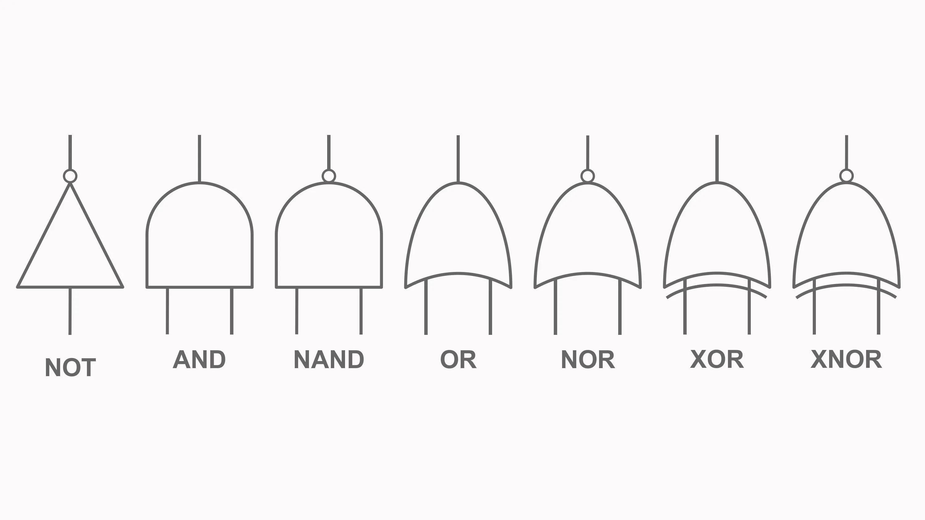
The small circle on a gate symbol represents inversion. For example:
- an AND symbol with an output circle is NAND;
- an OR symbol with an output circle is NOR;
- a circle on an input means that input is active-low.
What Is Combinational Logic?
A combinational logic circuit produces outputs determined by its current inputs.
It has no stored internal state. If the same stable inputs are applied again, the same outputs will be produced.
Examples of combinational circuits include:
- adders;
- subtractors;
- comparators;
- multiplexers;
- decoders;
- encoders;
- shifters.
The output does not change infinitely fast. Real gates have propagation delay, so a new input takes a small amount of time to travel through the circuit. The term combinational means that the logical result does not depend on a remembered previous state.
Binary Addition Basics
Binary arithmetic follows the same column-by-column principle as decimal arithmetic, but each digit can only be 0 or 1.
The four possible additions of two single bits are:
0 + 0 = 0
0 + 1 = 1
1 + 0 = 1
1 + 1 = 10
The result 10 is binary for decimal two. It contains:
- a sum bit of
0; - a carry bit of
1.
This gives us the behaviour needed for a half-adder.
Building a Half-Adder
A half-adder adds two one-bit inputs, A and B.
It produces two outputs:
- Sum, the low-order result bit;
- Carry, the bit carried into the next binary position.
The half-adder truth table is:
A | B | Sum | Carry |
|---|---|---|---|
| 0 | 0 | 0 | 0 |
| 0 | 1 | 1 | 0 |
| 1 | 0 | 1 | 0 |
| 1 | 1 | 0 | 1 |
The Sum column matches XOR:
Sum = A XOR BThe Carry column matches AND:
Carry = A AND BA half-adder therefore requires:
- one XOR gate;
- one AND gate.

The half-adder is our first complete arithmetic circuit. Its limitation is that it cannot include a carry from a less significant bit.
Half-Adder vs Full-Adder
A full-adder adds three one-bit values:
- input
A; - input
B; - carry-in
C_in.
It produces:
- Sum;
- carry-out
C_out.
The full-adder truth table is:
A | B | C_in | Sum | C_out |
|---|---|---|---|---|
| 0 | 0 | 0 | 0 | 0 |
| 0 | 0 | 1 | 1 | 0 |
| 0 | 1 | 0 | 1 | 0 |
| 0 | 1 | 1 | 0 | 1 |
| 1 | 0 | 0 | 1 | 0 |
| 1 | 0 | 1 | 0 | 1 |
| 1 | 1 | 0 | 0 | 1 |
| 1 | 1 | 1 | 1 | 1 |
The Sum output is:
Sum = A XOR B XOR C_inThe carry-out is high when at least two of the three inputs are high:
C_out = (A AND B) OR (C_in AND (A XOR B))Building a Full-Adder from Two Half-Adders
A full-adder can be built from:
- two half-adders;
- one OR gate.
The process works as follows:
- The first half-adder adds
AandB. - The second half-adder adds the first sum to
C_in. - An OR gate combines the two carry results.
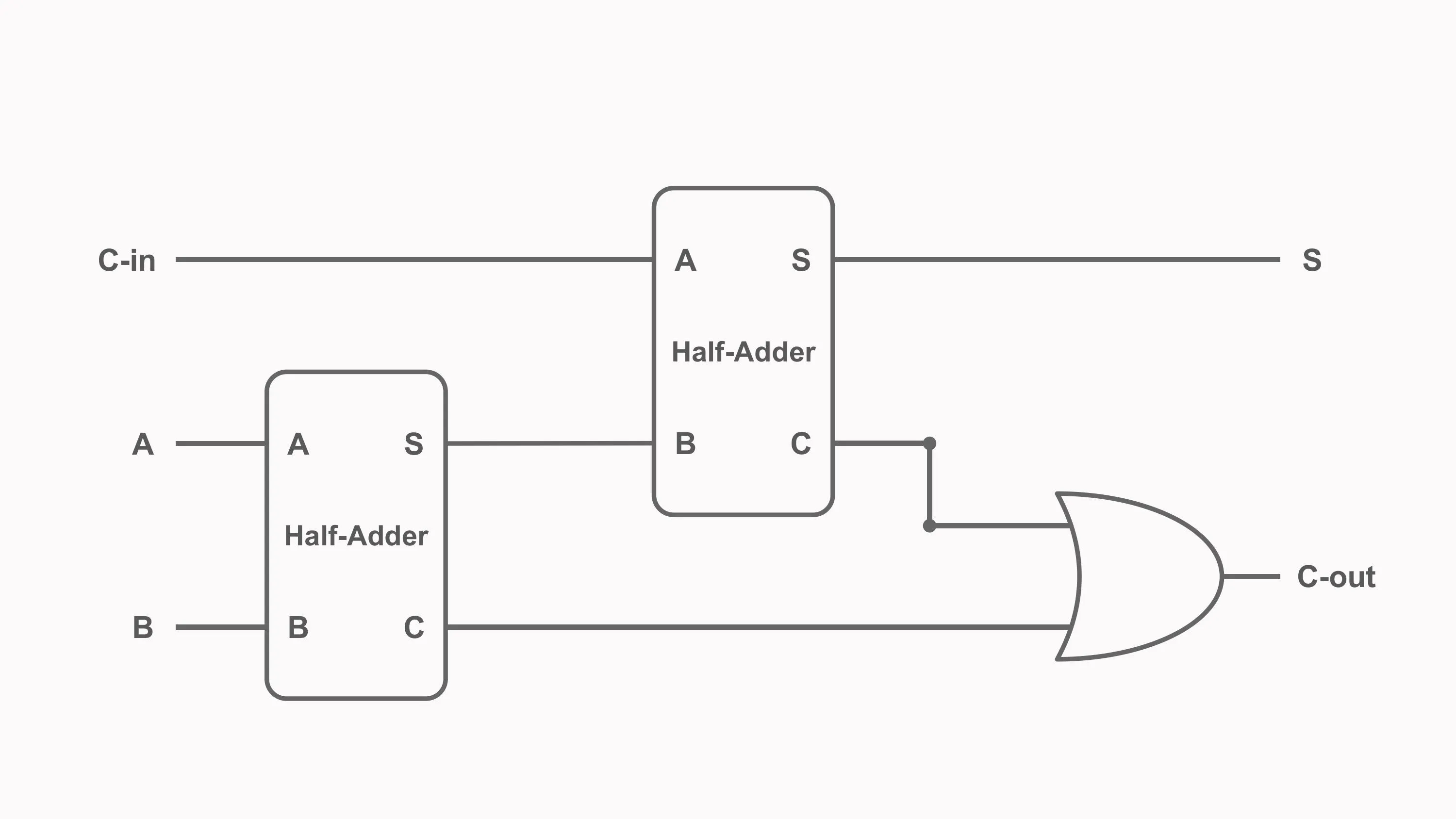
Suppose:
A = 1
B = 1
C_in = 1
The first half-adder calculates:
1 + 1 = 10Its intermediate sum is 0, and its carry is 1.
The second half-adder calculates:
0 + 1 = 1Its sum is 1, and its carry is 0.
The OR gate combines the carries:
1 OR 0 = 1The complete result is therefore:
C_out Sum = 11Binary 11 is decimal three, which is the correct result of 1 + 1 + 1.
Building an 8-Bit Ripple-Carry Adder
One full-adder handles one binary column. To add two 8-bit numbers, we can connect eight full-adders.
Each stage receives:
- one bit from input number
A; - one bit from input number
B; - a carry from the previous stage.
Each stage produces:
- one result bit;
- a carry for the next stage.
The least significant stage normally receives an initial carry-in of 0.

The carry travels from the least significant bit toward the most significant bit. Because it must pass through the stages one after another, this design is called a ripple-carry adder.
Example: Adding Two 8-Bit Numbers
Consider:
00001101 = 13
00011101 = 29
Adding them produces:
  00001101
+ 00011101
----------
  00101010
The binary result 00101010 is decimal 42.
Each full-adder solves one column and passes its carry to the next stage until all eight result bits are known.
Why Ripple-Carry Adders Can Be Slow
A ripple-carry adder is simple, but the most significant result may depend on a carry generated at the least significant position.
The carry cannot affect every stage at exactly the same instant. It must propagate through a chain of gates.
As the number of bits increases, the worst-case delay increases too. Faster processor designs therefore use alternatives such as:
- carry-lookahead adders;
- carry-select adders;
- prefix adders;
- other optimized carry networks.
The ripple-carry design remains an excellent starting point because it clearly demonstrates how larger arithmetic circuits are assembled from repeated one-bit components.
Carry-Out Is Not Always Overflow
The final carry-out has different meanings depending on how the bits are interpreted.
Unsigned Addition
For unsigned numbers, a final carry-out means the mathematical result requires one more bit than the available width.
For example, with four-bit unsigned values:
1111 + 0001 = 1 0000The four-bit result is 0000, and the extra 1 is the carry-out.
Signed Two’s-Complement Addition
For signed two’s-complement numbers, the final carry-out alone does not determine overflow.
Signed overflow occurs when:
- two positive numbers produce a negative-looking result; or
- two negative numbers produce a positive-looking result.
Another equivalent test compares the carry into the sign bit with the carry out of the sign bit. If those carry values differ, signed overflow occurred.
This distinction is important because a processor may expose separate status flags for carry and signed overflow.
From Combinational Logic to Sequential Logic
Combinational circuits transform current inputs into outputs, but they do not remember previous information.
A computer also needs circuits that can retain state. Examples include:
- registers holding operands;
- counters tracking progress;
- instruction-state machines;
- cache and memory structures;
- pipeline control signals.
Circuits whose behaviour depends on both current inputs and stored state are called sequential logic circuits.
Sequential circuits create memory through feedback: part of the output is connected back into the circuit so that a previous state can influence the next state.
What Is an SR Latch?
One of the simplest storage circuits is the SR latch.
S stands for set, and R stands for reset. The latch stores one bit and normally provides two outputs:
Q, the stored value;Q̅, the logical inverse ofQ.
Two cross-coupled NOR gates can form an active-high SR latch. Two cross-coupled NAND gates can form an active-low SR latch.
These versions look similar, but their input meanings and truth tables are different.
NAND-Based SR Latch
The diagram below uses cross-coupled NAND gates.
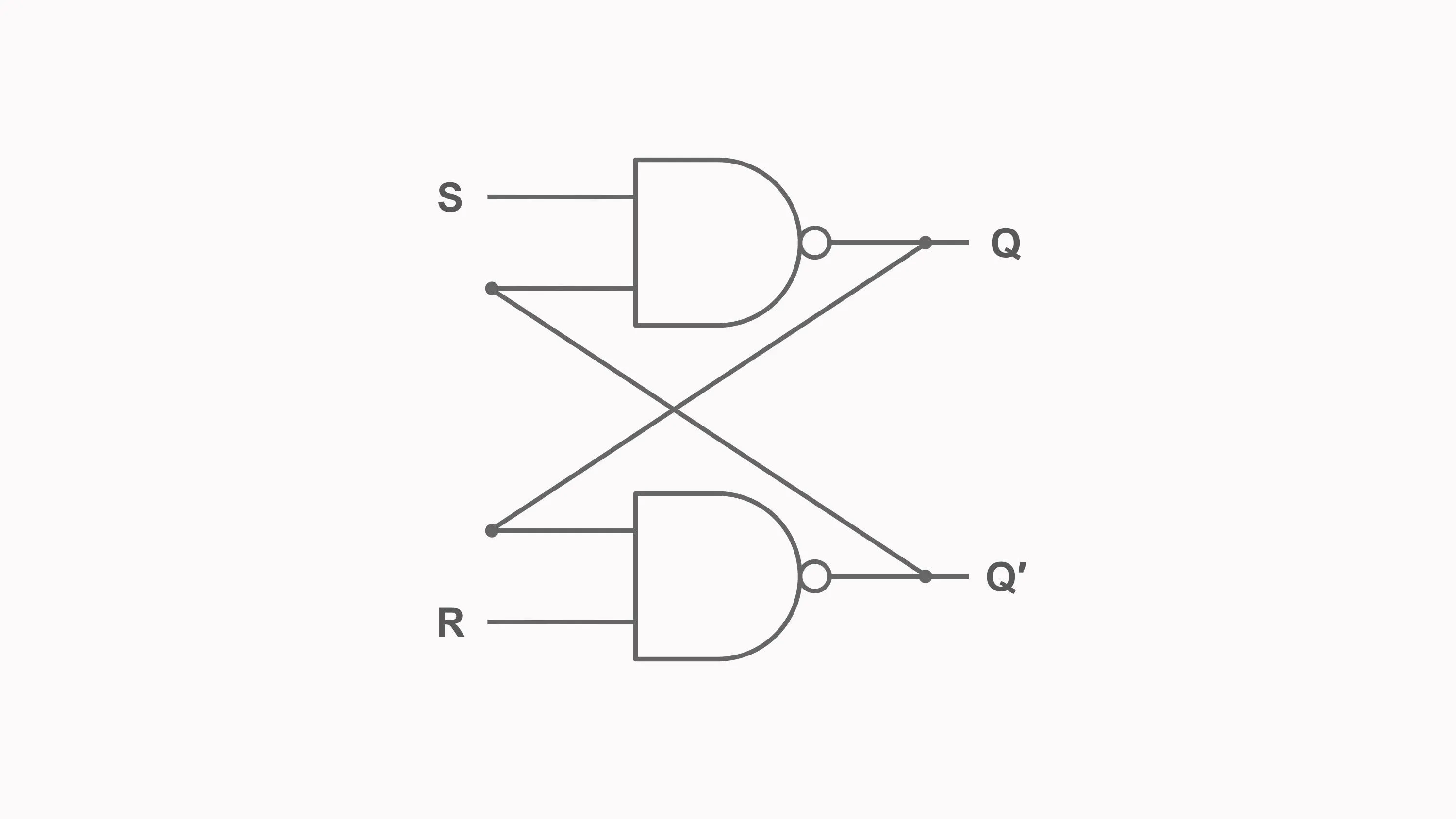
For a NAND-based SR latch, the inputs are active-low and are best written as S̅ and R̅.
S̅ = 0activates Set.R̅ = 0activates Reset.S̅ = 1andR̅ = 1hold the previous state.
Its truth table is:
S̅ | R̅ | Q next | Q̅ next | Meaning |
|---|---|---|---|---|
| 1 | 1 | Previous Q | Previous Q̅ | Hold |
| 0 | 1 | 1 | 0 | Set |
| 1 | 0 | 0 | 1 | Reset |
| 0 | 0 | 1 | 1 | Invalid input |
The hold condition demonstrates memory. When both inactive inputs are high, the feedback paths preserve the previously stored value.
The final row is invalid because both outputs become high, so they are no longer complements. Returning both inputs to the inactive state at nearly the same time can also make the final stored value unpredictable.
NOR-Based SR Latch
A NOR-based SR latch uses active-high inputs.
Its truth table is:
S | R | Q next | Q̅ next | Meaning |
|---|---|---|---|---|
| 0 | 0 | Previous Q | Previous Q̅ | Hold |
| 1 | 0 | 1 | 0 | Set |
| 0 | 1 | 0 | 1 | Reset |
| 1 | 1 | 0 | 0 | Invalid input |
This is the version commonly described with the simple rules:
- Set stores
1. - Reset stores
0. - Both low hold the previous value.
The active-high NOR table should not be mixed with a NAND-latch diagram, because the inactive and invalid input combinations are reversed.
Latch vs Flip-Flop
The terms latch and flip-flop are often used casually as though they mean the same thing, but there is an important distinction.
A latch is level-sensitive. It can respond while an enable signal is at its active level.
A flip-flop is normally edge-triggered. It captures input data at a clock transition, such as a rising or falling edge.
The two cross-coupled gates shown above form an SR latch, not a complete edge-triggered flip-flop.
More advanced storage elements include:
- gated SR latches;
- D latches;
- D flip-flops;
- JK flip-flops;
- T flip-flops.
Why D Flip-Flops Are Common
The invalid SR input combination is inconvenient. A D latch or D flip-flop avoids it by exposing one data input, D.
For a D flip-flop:
- the input value is sampled at the active clock edge;
- the sampled value appears at
Q; - the value remains stored until another active clock edge.
D flip-flops are widely used to build registers, counters, state machines, and processor pipelines because they provide predictable clock-controlled storage.
From One Stored Bit to a Register
One latch or flip-flop stores one bit.
Several flip-flops can be placed side by side to store a multi-bit value:
- eight flip-flops can form an 8-bit register;
- sixteen can form a 16-bit register;
- thirty-two can form a 32-bit register;
- sixty-four can form a 64-bit register.
A register may also include control logic for:
- loading a new value;
- preserving the old value;
- clearing its contents;
- shifting bits;
- selecting between several inputs.
This is how simple one-bit storage elements grow into the state-holding structures used throughout a processor.
Combinational vs Sequential Logic
The central difference is memory.
| Property | Combinational logic | Sequential logic |
|---|---|---|
| Output depends on | Current inputs | Current inputs and stored state |
| Remembers previous values | No | Yes |
| Feedback required | Not for logical function | Commonly used |
| Clock required | No | Often, but not always |
| Examples | Adders, multiplexers, decoders | Registers, counters, state machines |
An arithmetic logic unit contains a large amount of combinational logic. Processor registers and pipeline stages use sequential logic. A working CPU requires both.
Common Misconceptions
A Series Transistor Network Is Not Automatically an AND Gate
The logical result depends on where the output is measured and how the pull-up and pull-down networks are arranged. In static CMOS, series NMOS transistors naturally contribute to a NAND gate. An inverter is then added to obtain AND.
An OR Gate Is Not Ordinary Addition
Boolean OR uses the symbol +, but:
1 OR 1 = 1Ordinary arithmetic gives:
1 + 1 = 2Binary addition requires both a sum output and a carry output.
Combinational Outputs Do Not Change Instantly
Every gate has propagation delay. The output is determined only by current inputs once the signals have had enough time to settle.
Final Carry-Out Is Not the Same as Signed Overflow
Carry-out is directly useful for unsigned arithmetic. Signed two’s-complement overflow follows a different rule.
A Cross-Coupled NAND Pair Is an SR Latch
It is not, by itself, an edge-triggered flip-flop. It also uses active-low Set and Reset inputs.
Frequently Asked Questions
How do transistors form logic gates?
Transistors are arranged into pull-up and pull-down networks that connect an output toward a high or low voltage under specific input conditions. CMOS gates use complementary NMOS and PMOS networks to implement Boolean functions efficiently.
What is the difference between a half-adder and a full-adder?
A half-adder adds two input bits and produces Sum and Carry. A full-adder adds two input bits plus a carry-in, making it suitable for multi-bit addition.
How does an 8-bit adder work?
An 8-bit ripple-carry adder connects eight full-adders. Each stage adds one bit from each input number and receives the carry produced by the previous stage.
Why is it called a ripple-carry adder?
The carry signal moves, or ripples, from one full-adder to the next. The final stages must wait for earlier carry values to propagate.
Can an 8-bit adder produce a 9-bit result?
Yes. Adding two unsigned 8-bit numbers can require nine result bits. The eight Sum outputs provide the low eight bits, and the final carry-out provides the ninth bit.
What is sequential logic?
Sequential logic is digital logic whose behaviour depends on stored state as well as current inputs. Latches, flip-flops, registers, and counters are examples.
What is the difference between an SR latch and a D flip-flop?
An SR latch exposes separate Set and Reset controls and may have an invalid input combination. A D flip-flop samples one data input on a clock edge and stores it until the next active edge.
How many bits does one flip-flop store?
A basic flip-flop stores one binary bit. Multiple flip-flops are grouped to build wider registers.
Key Takeaways
Logic gates turn transistor switching behaviour into useful Boolean operations.
The main ideas are:
- NOT reverses a binary signal.
- AND is high only when all inputs are high.
- OR is high when at least one input is high.
- XOR is high when its inputs differ.
- NAND and NOR are universal gates.
- A half-adder uses XOR for Sum and AND for Carry.
- A full-adder includes a carry-in and can be chained into a multi-bit adder.
- An 8-bit ripple-carry adder uses eight full-adders.
- Unsigned carry-out and signed overflow represent different conditions.
- Feedback allows a latch to preserve one bit of state.
- A latch is level-sensitive, while a flip-flop is generally edge-triggered.
- Registers are built by combining multiple one-bit storage elements.
We have now moved from individual transistors to logic gates, arithmetic circuits, and basic memory. The next step is to use these components to build larger processor structures that can store values, select operations, and move data through a computer.